| CPC H10B 43/27 (2023.02) [H01L 21/67178 (2013.01); H01L 21/823487 (2013.01); H01L 29/40117 (2019.08); H10B 43/35 (2023.02); H01L 2924/1438 (2013.01)] | 18 Claims |
|
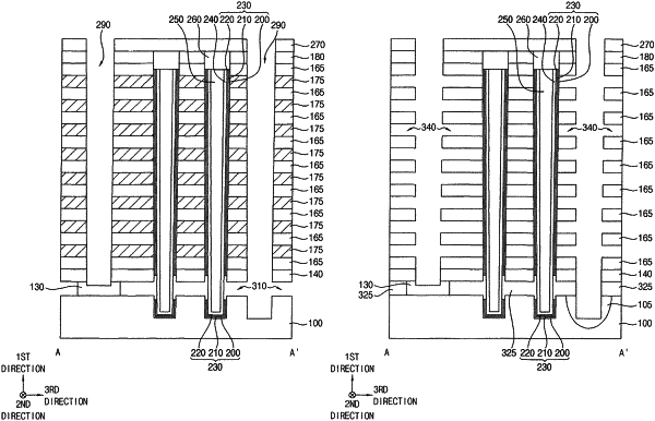
1. A stacked structure for a vertical memory device, the stacked structure comprising:
a first structure on a substrate, the first structure including a first sacrificial layer and a support layer stacked on the substrate in a vertical direction perpendicular to an upper surface of the substrate, the first sacrificial layer including germanium; and
a second structure on the first structure, the second structure including an insulation layer and a second sacrificial layer alternately and repeatedly stacked on the first structure, the second sacrificial layer including a nitride, such that the first sacrificial layer and the second sacrificial layer include different materials from each other,
wherein a thickness of the first structure in the vertical direction is less than a thickness of the second structure in the vertical direction.
|