| CPC H01L 27/10814 (2013.01) [H01L 27/10823 (2013.01); H01L 27/10852 (2013.01); H01L 27/10897 (2013.01)] | 15 Claims |
|
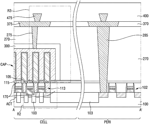
1. A semiconductor device comprising:
a lower electrode on a substrate;
a capacitor dielectric film extending on the lower electrode along a side surface of the lower electrode that is perpendicular to the substrate;
an upper electrode on the capacitor dielectric film and on the lower electrode;
an interface layer comprising a hydrogen blocking film and a hydrogen bypass film on the upper electrode, wherein the hydrogen bypass film comprises a conductive material;
an interlayer insulating film on the interface layer; and
a contact plug that penetrates the interlayer insulating film, the hydrogen blocking film and the hydrogen bypass film and is electrically connected to the upper electrode,
wherein the hydrogen blocking film comprises an insulating material without silicon,
wherein the hydrogen blocking film is between the upper electrode and the hydrogen bypass film,
wherein the hydrogen bypass film extends along the hydrogen blocking film, and
wherein the contact plug completely penetrates the hydrogen blocking film and contacts the upper electrode.
|