| CPC H10B 12/30 (2023.02) [H10B 12/03 (2023.02); H10B 12/05 (2023.02)] | 20 Claims |
|
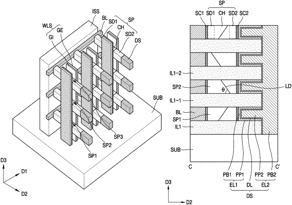
1. A semiconductor memory device comprising:
a first semiconductor pattern, and a second semiconductor pattern separated from the first semiconductor pattern in a vertical direction;
a first bit line electrically connected to a first source/drain region of the first semiconductor pattern, and a second bit line electrically connected to a first source/drain region of the second semiconductor pattern;
a word line structure in contact with the first semiconductor pattern and the second semiconductor pattern; and
a first data storage element electrically connected to a second source/drain region of the first semiconductor pattern, and a second data storage element electrically connected to a second source/drain region of the second semiconductor pattern,
wherein the first semiconductor pattern and the second semiconductor pattern are monocrystalline, and
wherein a crystal orientation of the first semiconductor pattern is different from a crystal orientation of the second semiconductor pattern,
wherein at least one of the first semiconductor pattern and the second semiconductor pattern includes a lattice defect extending to a bottom surface or top surface of the at least one of the first semiconductor pattern and the second semiconductor pattern.
|