| CPC H10B 12/053 (2023.02) [H10B 12/315 (2023.02); H10B 12/34 (2023.02); H10B 12/482 (2023.02)] | 20 Claims |
|
1. A method for manufacturing a semiconductor device, comprising:
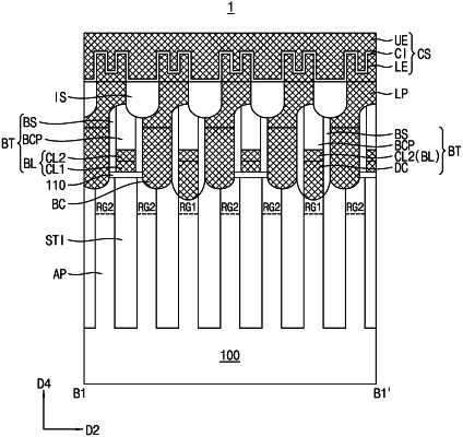
patterning a substrate, thereby forming an active pattern;
forming a trench penetrating the active pattern;
forming a support layer covering the trench;
forming a first opening at the support layer;
forming a gate electrode layer filling the trench through the first opening; and
forming a bit line structure electrically connected to the active pattern,
wherein the support layer comprises a base portion covering a top surface of the active pattern, and a support portion disposed in the trench.
|