| CPC H05K 3/284 (2013.01) [G01R 31/2818 (2013.01); H01L 2224/16225 (2013.01); H01L 2924/15311 (2013.01); H01L 2924/181 (2013.01)] | 13 Claims |
|
1. A method for fabricating an apparatus, the method comprising:
coupling one or more electronic components with a substrate or a printed circuit board;
coupling an electrical access port with the substrate or printed circuit board, the electrical access port including electrically conductive material; and
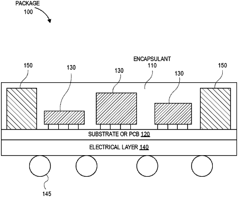
encapsulating the electrical access port with an encapsulant material, the encapsulant material having a top surface, a bottom surface, and side surfaces between the top surface and the bottom surface, wherein the bottom surface is on the substrate or printed circuit board, and wherein the encapsulant material has an opening in one of the side surfaces, the opening extending through the encapsulant material and exposing at least one of the electrical access port, wherein the electrical access port has a surface proximate the one of the side surfaces of the encapsulant material, and the opening exposes a portion of but not all of the surface of the electrical access port, wherein the electrical access port is electrically connected to one or more circuits of the apparatus.
|