| CPC H05K 1/024 (2013.01) [H05K 1/0219 (2013.01); H05K 3/4602 (2013.01); H05K 3/4655 (2013.01); H05K 2201/0723 (2013.01); H05K 2201/09063 (2013.01)] | 9 Claims |
|
1. A method for manufacturing a high-frequency circuit board comprising:
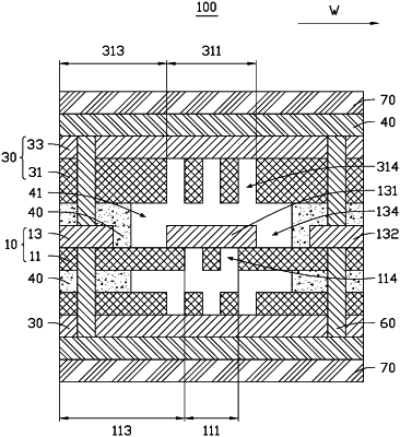
providing an inner circuit board including a first substrate layer and a first conductor layer on a surface of the first substrate layer, the first conductor layer including a signal line and two ground lines arranged at intervals on both sides of the signal line, the first substrate layer having a plurality of first through holes corresponding to the signal line;
providing two copper clad laminates, each of the two copper clad laminates comprising a second substrate layer and a copper foil on a surface of the second substrate layer, the second substrate layer having a plurality of second through holes;
pressing the two copper clad laminates on two sides of the inner circuit board, the second substrate layer abutting the inner circuit board, and the second through holes non-aligned with the first through holes; and
forming a second conductor layer from the copper foil.
|