| CPC H04N 25/704 (2023.01) [H01L 27/1463 (2013.01); H01L 27/14621 (2013.01); H01L 27/14627 (2013.01); H01L 27/14645 (2013.01); H04N 25/11 (2023.01); H04N 25/79 (2023.01)] | 20 Claims |
|
1. An image sensing device comprising:
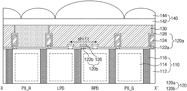
a pixel array including a plurality of image sensing pixels and phase detection pixel pairs disposed between the image sensing pixels, the plurality of image sensing pixels structured to detect incident light to generate first electrical signals carrying images in the incident light, the phase detection pixel pairs including phase detection pixels structured to generate second electrical signals for calculating a phase difference between the images,
wherein the pixel array includes:
a plurality of photoelectric conversion regions formed in a substrate to correspond to the image sensing pixels and the phase detection pixels;
a plurality of device isolation structures disposed in the substrate to isolate the photoelectric conversion regions from one another;
a plurality of color filters disposed over the substrate to correspond to the image sensing pixels and the phase detection pixel pairs;
a first grid structure disposed between a color filter of a first image sensing pixel, among the plurality of image sensing pixels, and a color filter of a first phase detection pixel pair adjacent to the first image sensing pixel from among the phase detection pixel pairs, and shifted by a first distance from a first device isolation structure, among the plurality of device isolation structures, disposed between a photoelectric conversion region of the first image sensing pixel and photoelectric conversion regions of the first phase detection pixel pair; and
a second grid structure disposed in the color filter of the first phase detection pixel pair, and shifted by a second distance different from the first distance from a second device isolation structure, among the plurality of device isolation structures, disposed between photoelectric conversion regions of the first phase detection pixel pair.
|