| CPC H04N 25/671 (2023.01) [H04N 17/002 (2013.01); H04N 25/50 (2023.01); H04N 25/77 (2023.01)] | 10 Claims |
|
1. A solid-state imaging element, comprising:
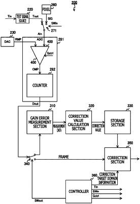
a test signal source configured to generate a test signal of a predetermined level;
an analog-to-digital converter configured to one of increase or decrease an analog signal according to an analog gain selected from among a plurality of analog gains, and convert the one of increased or decreased analog signal to a digital signal;
an input switching section configured to input, as the analog signal, either the test signal or a pixel signal to the analog-to-digital converter;
a correction value calculation section configured to obtain, based on the test signal and the digital signal, a correction value for correcting an error in the selected analog gain, and output the correction value; and
a correction section configured to correct the digital signal according to the outputted correction value.
|