| CPC H03M 1/145 (2013.01) [H03M 1/0612 (2013.01); H03M 1/164 (2013.01)] | 20 Claims |
|
1. An analog-to-digital converter (ADC), comprising:
an input terminal configured to receive an analog input voltage;
a first sub-ADC stage coupled to the input terminal and configured to sample the analog input voltage in response to a first phase clock signal and output a first digital value corresponding to the analog input voltage in response to a second phase clock signal;
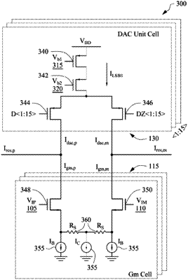
a current mode digital-to-analog converter (DAC) stage including
a transconductance amplifier (Gm) connected to the input terminal, the transconductance amplifier having a first plurality of transconductance amplifier cells, the transconductance amplifier configured to sample the analog input voltage in response to the first phase clock signal and convert the analog input voltage to a first current signal,
a current mode DAC connected to a sub-ADC output terminal of the first sub-ADC stage, the current mode DAC having a second plurality of current mode DAC unit cells and configured to convert the first digital value to a second current signal,
the current mode DAC stage configured to determine a residue current signal representing a difference between the first current signal and the second current signal, and convert the residue current signal to an analog residual voltage signal;
a second ADC stage coupled to the current mode DAC stage to receive the analog residual voltage signal, and convert the analog residue voltage signal to a second digital value;
an alignment and digital error correction stage configured to combine the first and the second digital values into a digital output voltage; and
an output terminal coupled to the alignment and error correction stage configured to output the digital output voltage.
|