US 11,700,005 B2
Phase locked loop generating adaptive driving voltage and related operating method
Kangyeop Choo, Hwaseong-si (KR); Insung Kim, Hwaseong-si (KR); Wooseok Kim, Suwon-si (KR); Taeik Kim, Seongnam-si (KR); Sunghyuck Lee, Hwaseong-si (KR); and Chanyoung Jeong, Hwaseong-si (KR)
Assigned to Samsung Electronics Co., Ltd., Suwon-si (KR)
Filed by SAMSUNG ELECTRONICS CO., LTD., Suwon-si (KR)
Filed on Oct. 25, 2021, as Appl. No. 17/509,540.
Claims priority of application No. 10-2021-0052528 (KR), filed on Apr. 22, 2021.
Prior Publication US 2022/0345137 A1, Oct. 27, 2022
Int. Cl. H03L 7/089 (2006.01); H03L 7/10 (2006.01)
CPC H03L 7/0891 (2013.01) [H03L 7/101 (2013.01)] 20 Claims
OG exemplary drawing
 
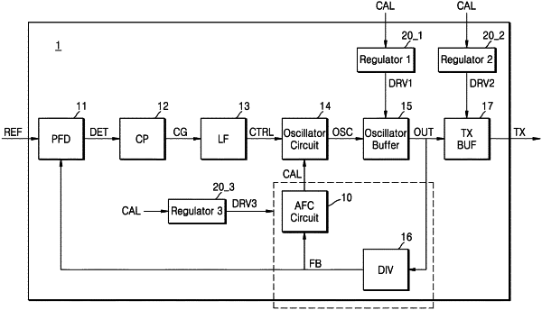
1. A phase locked loop (PLL) circuit, comprising:
a load circuit that generates an output signal in response to a driving voltage;
a frequency calibration circuit that generates a calibration signal in response to an output frequency of the output signal and a target frequency; and
a regulator that generates the driving voltage in response to the calibration signal.