| CPC H03K 3/0372 (2013.01) [H01L 23/5226 (2013.01); H01L 23/5286 (2013.01); H01L 27/0207 (2013.01); H01L 27/0924 (2013.01); H01L 29/0673 (2013.01); H01L 29/42392 (2013.01)] | 13 Claims |
|
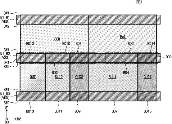
1. A semiconductor device including a flip flop cell, the flip flop cell formed on a semiconductor substrate and including a flip flop circuit, and the flip flop cell comprising:
active regions extending lengthwise in a first direction, from a plan view;
gate electrodes extending lengthwise in a second direction perpendicular to the first direction, from the plan view;
a power line extending lengthwise in the first direction, from the plan view;
a clock driver circuit;
a scan MUX circuit formed in a first continuously-bounded area of the flip flop cell from the plan view such that the scan MUX circuit generates a scan MUX circuit output, the first continuously-bounded area having a quadrilateral shape;
a master latch circuit formed in a second continuously-bounded area of the flip flop cell from the plan view, the master latch circuit formed to be adjacent to the scan MUX circuit in the first direction and connected to receive the scan MUX circuit output from the scan MUX circuit and output a master latch circuit output;
the clock driver circuit formed in at least a third continuously-bounded area of the flip flop cell from the plan view, the third continuously-bounded area partly overlapping the first continuously-bounded area in a first overlap region where the power line is disposed, and partly not overlapping the first continuously-bounded area, such that a first part of the scan mux circuit in the first overlap region overlaps and is shared with a first part of the clock driver circuit in the first overlap region, a second part of the scan mux circuit that is not shared with and does not overlap the clock driver circuit is adjacent to the power line in the second direction, and a second part of the clock driver circuit is adjacent to the power line on an opposite side of the power line as the second part of the scan mux circuit in the second direction;
a slave latch circuit formed in a fourth continuously-bounded area of the flip flop cell from the plan view and a fifth continuously-bounded area of the flip flop cell separate from the fourth continuously-bounded area, and connected to receive the master latch circuit output and output a slave latch circuit output, the fourth continuously-bounded area partly overlapping the first continuously-bounded area in a second overlap region where the power line is disposed; and
an output circuit formed in a sixth continuously-bounded area of the flip flop cell from a plan view and connected to receive the slave latch circuit output and to output an output signal to an outside of the flip flop,
wherein each of the scan mux circuit, the master latch circuit, the slave latch circuit, the clock driver circuit, and the output circuit:
consists of a plurality of active devices which together output a resulting signal for that circuit based on inputs, and
is a sub-circuit of the flip flop circuit,
wherein:
a first set of devices of the plurality of active devices which together output the slave latch circuit output for the slave latch circuit is located in the fourth continuously-bounded area,
the remainder of the devices of the plurality of active devices which together output the slave latch circuit output for the slave latch circuit are located in the fifth continuously-bounded area,
the third continuously-bounded area is located between the fourth continuously-bounded area and the fifth continuously-bounded area in the first direction,
the slave latch circuit consists of two continuously-bounded areas each having a rectangular shape, and
the clock driver circuit consists of one or two continuously-bounded areas, each having a rectangular shape.
|