US 11,699,985 B2
Layered body, and saw device
Keiichirou Geshi, Osaka (JP); Masato Hasegawa, Osaka (JP); and Shigeru Nakayama, Osaka (JP)
Assigned to SUMITOMO ELECTRIC INDUSTRIES, LTD., Osaka (JP)
Appl. No. 16/754,779
Filed by SUMITOMO ELECTRIC INDUSTRIES, LTD., Osaka (JP)
PCT Filed Sep. 21, 2018, PCT No. PCT/JP2018/034964
§ 371(c)(1), (2) Date Apr. 9, 2020,
PCT Pub. No. WO2019/073783, PCT Pub. Date Apr. 18, 2019.
Claims priority of application No. 2017-198780 (JP), filed on Oct. 12, 2017.
Prior Publication US 2020/0304099 A1, Sep. 24, 2020
Int. Cl. H03H 9/25 (2006.01); H03H 9/08 (2006.01); H03H 9/02 (2006.01); H03H 9/145 (2006.01)
CPC H03H 9/08 (2013.01) [H03H 9/02559 (2013.01); H03H 9/02574 (2013.01); H03H 9/145 (2013.01); H03H 9/25 (2013.01)] 8 Claims
OG exemplary drawing
 
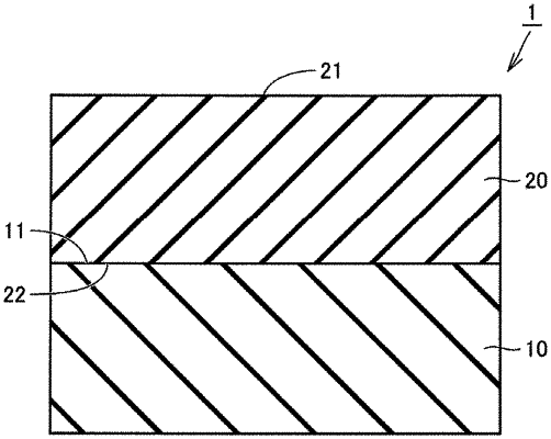
1. A layered body comprising:
a ceramic substrate formed of polycrystalline ceramic and having a supporting main surface; and
a piezoelectric substrate formed of a piezoelectric material and having a bonding main surface in contact with the supporting main surface of the ceramic substrate,
wherein at the supporting main surface, a mean of grain sizes of the polycrystalline ceramic is 15 μm or more and less than 40 μm, and
a standard deviation of the grain sizes is less than 1.5 times the mean.