| CPC H03H 9/02133 (2013.01) [H03H 3/02 (2013.01); H03H 9/0509 (2013.01); H03H 9/1021 (2013.01); H03H 9/19 (2013.01); H03H 2003/022 (2013.01)] | 7 Claims |
|
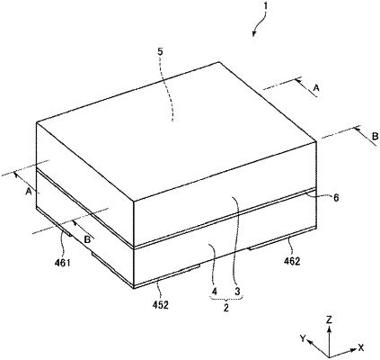
1. A vibrator device comprising:
a base having
a semiconductor substrate composed of silicon including a first surface and a second surface in a front-back relationship with the first surface, and includes a semiconductor circuit having an active surface on the first surface side or the second surface side of the semiconductor substrate,
a first insulating layer which is a film made of silicon oxide disposed on the first surface,
a first internal terminal and a second internal terminal placed on the first insulating layer,
a second insulating layer which is a film made of silicon oxide disposed on the second surface and divided into a plurality of regions including a first external terminal region and a second external terminal region separated from the first external terminal region,
a first external terminal placed in the first external terminal region and electrically coupled to the first internal terminal, and
a second external terminal placed in the second external terminal region and electrically coupled to the second internal terminal;
a vibrator element placed on the first surface and electrically coupled to the first internal terminal and the second internal terminal; and
a lid bonded to the first surface and housing the vibrator element between the base and itself, wherein
the base has an insulating layer non-formation region having no insulating layer on the second surface of the semiconductor substrate,
the semiconductor substrate has a rectangular shape in a plan view;
the insulating layer non-formation region has a first portion disposed from a first side contained in an outer edge of the semiconductor substrate to a second side facing the first side in the plan view, and
the first external terminal region and the second external terminal region are separated by the first portion of the insulating layer non-formation region.
|