| CPC H01S 5/023 (2021.01) [H01S 5/0237 (2021.01); H01S 5/02469 (2013.01)] | 4 Claims |
|
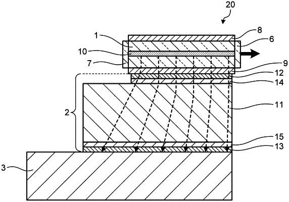
1. A semiconductor laser machine comprising:
a semiconductor laser element including a first end face adapted to emit a laser beam and a second end face that is opposite the first end face;
a heat sink; and
a sub-mount adapted to fix the semiconductor laser element to the heat sink, wherein
the sub-mount includes:
a substrate adapted to relieve thermal stress;
a solder layer joined to the semiconductor laser element; and
a junction layer formed between the substrate and the solder layer,
compared with the semiconductor laser element, the substrate is extended in a rearward direction that is from the first end face toward the second end face, and
the solder layer and the junction layer are removed behind the second end face, wherein
the solder layer and the junction layer have respective rear edges positioned forwardly of the second end face, and
a front edge of the solder layer and a front edge of the junction layer are aligned with a front end face of the substrate.
|