| CPC H01Q 1/2283 (2013.01) [H01L 23/66 (2013.01); H01L 24/17 (2013.01); H01L 24/95 (2013.01); H01Q 9/0421 (2013.01); H01Q 21/0087 (2013.01); H01Q 21/065 (2013.01); H01L 2223/6677 (2013.01); H01L 2924/014 (2013.01)] | 10 Claims |
|
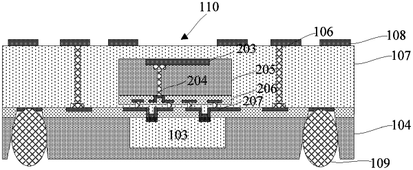
1. An antenna package structure, comprising:
an antenna circuit chip;
a first packaging layer, disposed on the antenna chip, wherein the first packaging layer comprises a first surface and a second surface opposite to the first surface, wherein two ports on a front surface of the antenna chip are exposed from the first surface;
a first rewiring layer, formed on the first surface of the first packaging layer, wherein the first rewiring layer comprises a first surface connected to the two ports of the antenna chip, wherein a second surface is opposite to the first surface;
an antenna structure, comprising a second packaging layer, a first antenna metal layer, a second rewiring layer, and a first metal bump, wherein the first antenna metal layer is disposed on a first surface of the second packaging layer, wherein the second rewiring layer is disposed on a second surface of the second packaging layer, wherein the first antenna metal layer is electrically connected to the second rewiring layer by a first metal connecting column passing through the second packaging layer, the first metal bump is formed on the second rewiring layer, and bonded to the first metal wiring layer of the first rewiring layer;
a second metal connecting column, formed on the second surface of the first rewiring layer, wherein the second metal connecting column is taller than a top surface of the antenna structure;
a third packaging layer, disposed on the antenna structure, wherein a top surface of the second metal connecting column is exposed from the third packaging layer;
a second antenna metal layer, formed on a top surface of the third packaging layer, wherein the second antenna metal layer is patterned to connect to the second metal connecting column; and
a second metal bump, formed in a via hole in the first packaging layer, and electrically connected to the first surface of the first rewiring layer.
|