| CPC H01L 33/56 (2013.01) [H01L 33/0095 (2013.01); H01L 2933/005 (2013.01)] | 13 Claims |
|
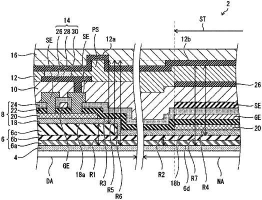
1. A display device comprising:
an underlayer, a first insulating film contacting an upper face of the underlayer, a semiconductor layer, a second insulating film, a first metal layer, a first resin layer, a first electrode, and a second resin layer, which are formed in order from bottom to top,
wherein any one of the underlayer, the first resin layer, and the second resin layer is a thin film layer having a first maximum film thickness in a display region that is thicker than a second maximum film thickness of a corresponding one of the underlayer, the first resin layer, and the second resin layer in a frame region, and the frame region surrounds the display region, and
wherein the underlayer includes a resin layer, and the display region is provided with a light-emitting element.
|