| CPC H01L 33/387 (2013.01) [H01L 33/20 (2013.01); H01L 33/24 (2013.01); H01L 33/38 (2013.01); H01L 33/44 (2013.01); H01L 33/46 (2013.01); H01L 33/54 (2013.01); H01L 33/62 (2013.01); H01L 2224/73265 (2013.01)] | 18 Claims |
|
1. A light-emitting element, comprising:
a substrate comprising:
a first side;
a second side opposite to the first side; and
a third side connecting the first side and the second side;
a light-emitting semiconductor stack formed on the substrate and comprising:
a first semiconductor layer;
a second semiconductor layer; and
a light-emitting layer between the first semiconductor layer and the second semiconductor layer;
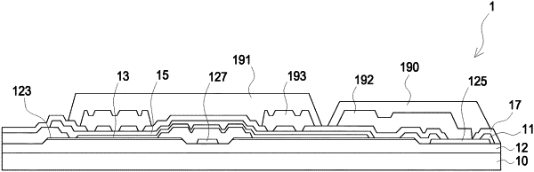
a first electrode formed on the first semiconductor layer, extending from the first side to the second side and comprising a contact area and a first extension area;
a second electrode formed on the second semiconductor layer;
a protection layer formed on the light-emitting semiconductor stack, comprising a first through hole exposing the first electrode and a second through hole exposing the second electrode;
a first conductive part formed on the protection layer and electrically connected to the first electrode through the first through hole; and
a second conductive part formed on the protection layer and electrically connected to the second electrode through the second through hole, wherein the second conductive part comprises a projected area on the light-emitting semiconductor stack, the first extension area is located outside the projected area and located between the second conductive part and the third side,
wherein the first conductive part and the second conductive part each comprises a concave-convex profile.
|