| CPC H01L 33/24 (2013.01) [H01L 25/0753 (2013.01); H01L 33/32 (2013.01); H01L 33/0075 (2013.01)] | 23 Claims |

|
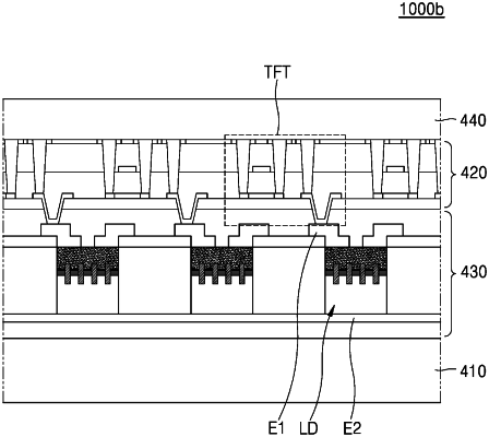
1. A light emitting diode (LED) comprising:
a first semiconductor layer;
a plurality of active elements disposed on the first semiconductor layer, each of the plurality of active elements spaced apart from each other and having a width less than a width of the first semiconductor layer; and
a second semiconductor layer disposed on the plurality of active elements and comprises a material different from that the first semiconductor layer,
wherein the first semiconductor layer comprises a first semiconductor common layer and a plurality of first semiconductor elements respectively in contact with both the plurality of active elements and the first semiconductor common layer, the plurality of first semiconductor elements being spaced apart from each other,
wherein the second semiconductor layer comprises a plurality of second semiconductor elements respectively in contact with the plurality of active elements, the plurality of second semiconductor elements being spaced apart from each other, and
wherein the first semiconductor common layer and the plurality of first semiconductor elements are made of the same material.
|