| CPC H01L 29/86 (2013.01) [H10B 69/00 (2023.02); H10K 10/50 (2023.02); H10K 19/00 (2023.02); H10K 19/201 (2023.02)] | 25 Claims |
|
1. A semiconductor device, comprising:
a first electrode;
a second electrode isolated from direct contact with the first electrode;
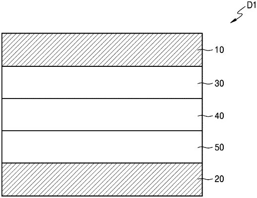
a ferroelectric layer;
a conductive metal oxide layer; and
a semiconductor layer,
wherein the ferroelectric layer, the conductive metal oxide layer, and the semiconductor layer are between the first electrode and the second electrode, and
wherein a difference in lattice constant between the conductive metal oxide layer and the ferroelectric layer is equal to or less than 10%.
|
|
21. The semiconductor apparatus of claim 19, wherein the cell string includes a plurality of cell strings isolated from direct contact with each other along a plane of the stack structure, wherein the vertical direction is perpendicular to the plane of the stack structure.
|
|
24. A semiconductor device, comprising:
a memory element that is configured to store information, the memory element including a ferroelectric layer;
a selection element electrically connected to the memory element, the selection element configured to perform selection of the semiconductor device based on controlling a flow of an electric current through the memory element, the selection element including a semiconductor layer; and
a conductive metal oxide layer,
wherein the ferroelectric layer and the semiconductor layer are coupled to each other between two electrodes, and no terminals are between the ferroelectric layer and the semiconductor layer, and wherein a difference in lattice constant between the conductive metal oxide layer and the ferroelectric layer is equal to or less than 10%.
|