|
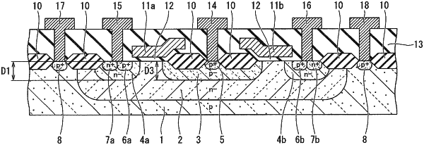
1. A semiconductor device comprising: a semiconductor layer of a first conductivity-type; a well region of a second conductivity-type provided at an upper part of the semiconductor layer; a base region of the second conductivity-type provided at an upper part of the well region and having an impurity concentration higher than an impurity concentration of the well region; a carrier supply region of the first conductivity-type provided at an upper part of the base region; a drift region of the first conductivity-type provided at the upper part of the well region separately from the base region; a carrier reception region of the first conductivity-type provided at an upper part of the drift region and having an impurity concentration higher than an impurity concentration of the drift region; a gate electrode provided on a top surface of the well region interposed between the base region and the drift region via a gate insulating film; and a punch-through prevention region of the second conductivity-type provided at the upper part of the well region and having an impurity concentration higher than the impurity concentration of the well region and different from the impurity concentration of the base region.
|