| CPC H01L 29/78696 (2013.01) [G11C 11/419 (2013.01); H01L 21/02603 (2013.01); H01L 21/02606 (2013.01); H01L 27/14616 (2013.01); H01L 29/0665 (2013.01); H01L 29/0669 (2013.01); H01L 29/0673 (2013.01); H01L 29/1025 (2013.01); H01L 29/42392 (2013.01); H01L 29/66795 (2013.01); H10B 10/12 (2023.02); H01L 29/1037 (2013.01); H01L 29/66787 (2013.01); H01L 29/785 (2013.01); H10B 43/20 (2023.02)] | 18 Claims |
|
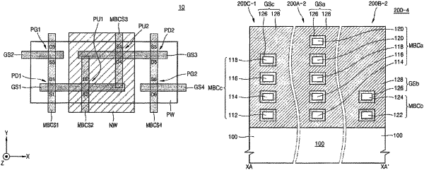
1. A semiconductor device, comprising:
first to third multi-bridge channel structures arranged in a second direction and sequentially spaced apart from one another in a first direction that is substantially perpendicular to the second direction;
a first gate structure arranged in the first direction, the first gate structure surrounding the first multi-bridge channel structure;
a first source and drain region located in the first multi-bridge channel structure on respective sides of the first gate structure;
a second gate structure arranged in the first direction and spaced apart from the first gate structure in the first direction, the second gate structure surrounding the second and third multi-bridge channel structures;
second and third source and drain regions located in the second and third multi-bridge channel structures on respective sides of the second gate structure;
a third gate structure spaced apart from the second gate structure in the second direction and spaced apart from the first gate structure in the first direction, the third gate structure surrounding the third multi-bridge channel structure;
a fourth source and drain region located in the third multi-bridge channel structure on respective sides of the third gate structure;
wherein the first to third multi-bridge channel structures are surrounded with the first to third gate structures, respectively, and each of the first to third multi-bridge channel structures comprises a plurality of nano-bridges serving as channels, the plurality of nano-bridges stacked apart from one another in a third direction that is substantially perpendicular to a plane defined by the first direction and the second direction,
at least one of the first to third multi-bridge channel structures respectively surrounded by the first to third gate structures comprises a different number of nano-bridges from the other multi-bridge channel structures, and
each of the plurality of nano-bridges in the first to third multi-bridge channel structures is formed of a nano-sheet, and wherein a length of the nano-sheet in the second direction is greater than a length of the nano-sheet in the first direction.
|