| CPC H01L 29/7869 (2013.01) [H01L 27/1225 (2013.01); H01L 27/1255 (2013.01); H01L 27/14609 (2013.01); H01L 27/14612 (2013.01); H01L 27/14634 (2013.01); H01L 29/4908 (2013.01); H01L 29/78603 (2013.01); H01L 29/78645 (2013.01); H01L 29/78648 (2013.01); H01L 29/78696 (2013.01); H10K 59/1216 (2023.02)] | 5 Claims |
|
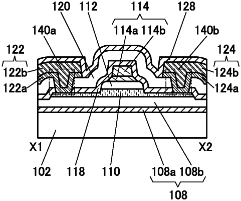
1. A transistor comprising:
an island-shaped oxide semiconductor film;
a single-layer gate insulating film over the island-shaped oxide semiconductor film; and
a gate electrode over the single-layer gate insulating film,
wherein, in a cross-sectional view parallel to a channel length direction of the transistor, an edge of the single-layer gate insulating film is located on a top surface of the island-shaped oxide semiconductor film,
wherein a first insulating film comprising a region in contact with a side surface of the gate electrode, a region in contact with a top surface of the single-layer gate insulating film, and a region in contact with the top surface of the island-shaped oxide semiconductor film, is provided,
wherein the top surface of the single-layer gate insulating film comprises a region projecting from the gate electrode,
wherein the transistor is a top-gate transistor,
wherein, in the cross-sectional view, the island-shaped oxide semiconductor film comprises a first region overlapping with the single-layer gate insulating film and a second region not overlapping with the single-layer gate insulating film, the second region having a smaller thickness than the first region, and
wherein at least one of a source electrode and a drain electrode comprises a region in contact with a top surface of the second region.
|