| CPC H01L 29/785 (2013.01) [H01L 21/823431 (2013.01); H01L 27/0886 (2013.01); H01L 29/42392 (2013.01); H01L 29/66545 (2013.01); H01L 29/66795 (2013.01)] | 20 Claims |
|
1. An integrated circuit device comprising:
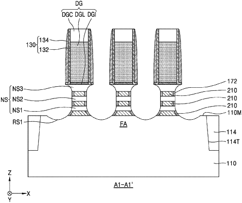
a fin shaped active region protruding from a substrate and extending in a first direction;
first, second, and third semiconductor patterns on the fin shaped active region, the first to third semiconductor patterns being spaced apart from each other in a vertical direction;
a gate electrode surrounding the first to third semiconductor patterns and extending in a second direction that is perpendicular to the first direction, the gate electrode comprising:
a main gate portion extending on the third semiconductor pattern in the second direction;
a first sub-gate portion between the fin shaped active region and the first semiconductor pattern;
a second sub-gate portion between the first semiconductor pattern and the second semiconductor pattern; and
a third sub-gate portion between the second semiconductor pattern and the third semiconductor pattern, the third sub-gate portion comprising a sub-gate center portion, and sub-gate edge portions comprising opposing end portions of the third sub-gate portion, respectively, in the second direction;
source/drain regions on opposing sides of the first to third semiconductor patterns, respectively, the source/drain regions being connected to the first to third semiconductor patterns; and
a plurality of inner spacers between side surfaces of the first to third sub-gate portions and the source/drain regions,
wherein, in a horizontal cross-sectional view, a first width of the sub-gate center portion in the first direction is less than a second width of one of the sub-gate edge portions in the first direction, and
wherein a third width of the third sub-gate portion in the first direction is less than a fourth width of the first sub-gate portion in the first direction.
|