| CPC H01L 29/7848 (2013.01) [H01L 21/26506 (2013.01); H01L 21/26513 (2013.01); H01L 21/324 (2013.01); H01L 21/707 (2013.01); H01L 21/823807 (2013.01); H01L 21/823814 (2013.01); H01L 21/84 (2013.01); H01L 27/1203 (2013.01); H01L 29/161 (2013.01); H01L 29/1608 (2013.01); H01L 29/66628 (2013.01); H01L 29/66772 (2013.01); H01L 29/165 (2013.01); H01L 29/66795 (2013.01)] | 10 Claims |

|
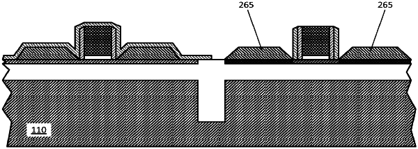
1. A device, comprising:
a substrate;
an insulating layer on the substrate;
an ultrathin semiconductor layer on the insulating layer, the ultrathin semiconductor layer having a first surface and a second surface opposite the first surface, the ultrathin semiconductor layer including:
a first portion including a conductivity dopant between the first and second surface of the ultrathin semiconductor layer, the first portion having a first doping level;
a second portion laterally adjacent to the first portion and including the conductivity dopant between the first and second surface of the ultrathin semiconductor layer, the second portion having a second doping level that is different than the first doping level; and
a third portion laterally adjacent to the first portion and including the conductivity dopant between the first and second surface of the ultrathin semiconductor layer, the first portion being between the second portion and the third portion, the third portion having a third doping level that is different than the first doping level; and
a transistor on the ultrathin semiconductor layer, the transistor including a channel that is at least a part of the first portion of the ultrathin semiconductor layer,
wherein the ultrathin semiconductor layer includes gallium and the conductivity dopant includes nitrogen.
|