| CPC H01L 29/7846 (2013.01) [H01L 29/167 (2013.01); H01L 29/41791 (2013.01); H01L 29/42364 (2013.01)] | 20 Claims |

|
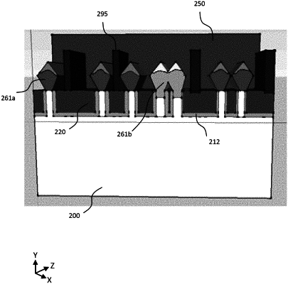
1. An integrated circuit (IC) comprising:
a body of semiconductor material, the semiconductor material comprising germanium;
a gate structure on the body, the gate structure including a gate dielectric and a gate electrode, and the gate structure having a gate-all-around (GAA) configuration on the body of semiconductor material;
a source region and a drain region both adjacent to the body such that the body is between the source and drain regions, at least one of the source region and the drain region including n-type impurity;
a shallow trench isolation (STI) region adjacent the at least one of the source region and the drain region; and
a layer of insulation material between the at least one of the source region and the drain region and the STI region, wherein the layer of insulation material is distinct from the STI region, and wherein the layer of insulation material comprises silicon, oxygen and carbon.
|