| CPC H01L 29/7842 (2013.01) | 14 Claims |
|
1. A semiconductor processing method comprising:
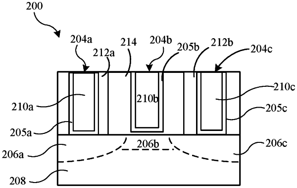
depositing a stressed material on an adjacent layer, wherein the adjacent layer is disposed between and in contact with each of the stressed material and a substrate comprising doped source and drain regions, and wherein the adjacent layer is characterized by an increased stress level after the deposition of the stressed material, wherein the stressed material has a tensile stress greater than or about 4 GPa;
heating the stressed material and the adjacent layer; and
removing the stressed material from the adjacent layer, wherein the adjacent layer retains at least a portion of increased stress after the removal of the stressed material.
|