| CPC H01L 29/7827 (2013.01) [H01L 29/0653 (2013.01); H01L 29/401 (2013.01); H01L 29/42364 (2013.01); H01L 29/42368 (2013.01); H01L 29/513 (2013.01); H01L 29/517 (2013.01); H01L 29/518 (2013.01); H01L 29/66666 (2013.01)] | 20 Claims |
|
1. A method for manufacturing a vertical field effect transistor (VFET), the method comprising:
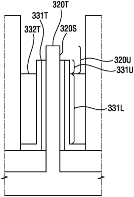
providing a stack of a bottom source/drain region, a fin structure, and a gate structure on a side wall of the fin structure, an interlayer on a sidewall of the gate structure, and a mask layer on the fin structure, the stack further comprising a bottom spacer on the bottom source/drain region and below the gate structure and the interlayer, and the gate structure comprising a gate dielectric layer on a sidewall of the fin structure and a conductor layer on the gate dielectric layer;
etching the stack from a top surface thereof to remove the gate dielectric layer and the conductor layer, by different depths from the top surface thereof, and the mask layer such that an upper portion of the gate dielectric layer is positioned above a plane where a top surface of the conductor layer is positioned; and
forming a top source/drain region on a top surface of the fin structure, a top surface of the gate structure and a sidewall of the interlayer.
|