| CPC H01L 29/7816 (2013.01) [H01L 21/823857 (2013.01); H01L 27/0922 (2013.01); H01L 29/0649 (2013.01); H01L 29/407 (2013.01); H01L 29/41758 (2013.01); H01L 29/4232 (2013.01); H01L 29/4236 (2013.01); H01L 29/42368 (2013.01); H01L 29/66681 (2013.01); H01L 29/66704 (2013.01); H01L 29/7825 (2013.01); H01L 29/7831 (2013.01); H01L 29/7835 (2013.01); H01L 29/0692 (2013.01)] | 14 Claims |
|
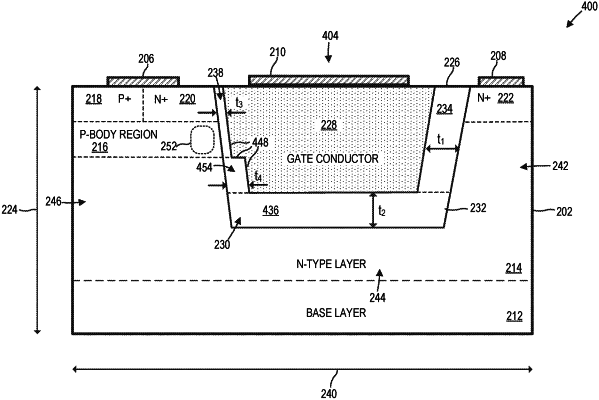
1. A lateral double-diffused metal-oxide-semiconductor (LDMOS) transistor, comprising:
silicon semiconductor structure, including:
a base layer,
an n-type layer disposed over the base layer in a thickness direction,
a p-body region disposed in the n-type layer,
a source p+ region and a source n+ region each disposed in the p-body region, and
a drain n+ region disposed in the n-type layer; and
a vertical gate including:
a gate conductor extending from a first outer surface of the silicon semiconductor structure into the silicon semiconductor structure into the n-type layer in the thickness direction and the gate conductor is disposed between the source n+ region and the drain n+ region in a lateral direction orthogonal to the thickness direction; and
a gate dielectric layer including at least four dielectric sections, each of the at least four dielectric sections separating the gate conductor from the silicon semiconductor structure by a respective separation distance, wherein the at least four dielectric sections include:
a first dielectric section separating the gate conductor from a drain portion of the n-type layer in the lateral direction by a first separation distance t1;
a second dielectric section separating the gate conductor from a well portion of the n-type layer in the thickness direction by a second separation distance t2 different from the first separation distance t1; and
a third dielectric section separating the gate conductor from the p-body region by a third separation distance t3 different from each of the first separation distance t1 and the second separation distance t2;
a fourth dielectric section separating the gate conductor from a source portion of the n-type layer in the lateral direction by a fourth separation distance t4 that is different from each of the first separation distance t1, the second separation distance t2, and the third separation distance t3.
|