| CPC H01L 29/7786 (2013.01) [H01L 23/291 (2013.01); H01L 23/3171 (2013.01); H01L 29/1066 (2013.01); H01L 29/2003 (2013.01); H01L 29/4236 (2013.01); H01L 29/66462 (2013.01); H01L 29/1087 (2013.01); H01L 29/207 (2013.01); H01L 29/41766 (2013.01); H01L 29/7378 (2013.01)] | 16 Claims |
|
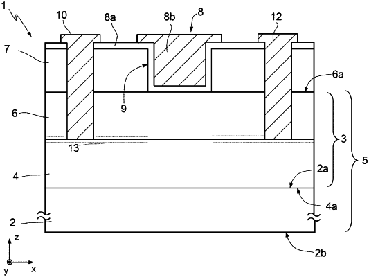
1. A structure comprising:
a first semiconductor layer of gallium nitride;
a second semiconductor layer of aluminum gallium nitride on the first semiconductor layer, the second semiconductor layer including a mole fraction of aluminum in a range of 5% and 20%, and a thickness in a range of 5 nm and 30 nm, the second semiconductor layer including a first region and a second region; and
an insulation layer in contact with the first region of the second semiconductor layer and absent from the second region of the second semiconductor layer, the insulation layer including a dielectric material that has a lattice mismatch with respect to the aluminum gallium nitride of the second semiconductor layer in a range of 1% and 20%;
a first source or drain structure extending through the insulation layer, the first source or drain structure terminates at an interface between the first semiconductor layer and the second semiconductor layer.
|