US 11,699,747 B2
Quantum dot devices with multiple layers of gate metal
Hubert C. George, Portland, OR (US); Sarah Atanasov, Beaverton, OR (US); Ravi Pillarisetty, Portland, OR (US); Lester Lampert, Portland, OR (US); James S. Clarke, Portland, OR (US); Nicole K. Thomas, Portland, OR (US); Roman Caudillo, Portland, OR (US); Kanwaljit Singh, Rotterdam (NL); David J. Michalak, Portland, OR (US); Jeanette M. Roberts, North Plains, OR (US); and Stephanie A. Bojarski, Beaverton, OR (US)
Assigned to Intel Corporation, Santa Clara, CA (US)
Filed by Intel Corporation, Santa Clara, CA (US)
Filed on Mar. 26, 2019, as Appl. No. 16/365,018.
Prior Publication US 2020/0312989 A1, Oct. 1, 2020
Int. Cl. H01L 29/423 (2006.01); G06N 10/00 (2022.01); H01L 29/66 (2006.01); H01L 29/78 (2006.01); H01L 29/40 (2006.01); H01L 29/76 (2006.01); B82Y 10/00 (2011.01); H01L 29/775 (2006.01)
CPC H01L 29/775 (2013.01) [B82Y 10/00 (2013.01); G06N 10/00 (2019.01); H01L 29/401 (2013.01); H01L 29/4236 (2013.01); H01L 29/66439 (2013.01); H01L 29/66977 (2013.01); H01L 29/7613 (2013.01); H01L 29/7831 (2013.01)] 19 Claims
OG exemplary drawing
 
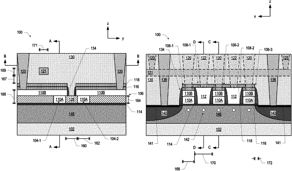
1. A quantum dot device, comprising:
a quantum well stack;
an insulating material above the quantum well stack, wherein the insulating material includes a trench; and
a gate, wherein the gate includes a first gate metal in the trench and a second gate metal above the first gate metal,
wherein at least one of:
the first gate metal and the second gate metal have different material compositions,
the first gate metal and the second gate metal have different microstructures, or
a seam is present between the first gate metal and the second gate metal.