| CPC H01L 29/66833 (2013.01) [H01L 21/31105 (2013.01); H01L 21/32139 (2013.01); H01L 29/66666 (2013.01); H10B 41/27 (2023.02); H10B 43/27 (2023.02)] | 10 Claims |
|
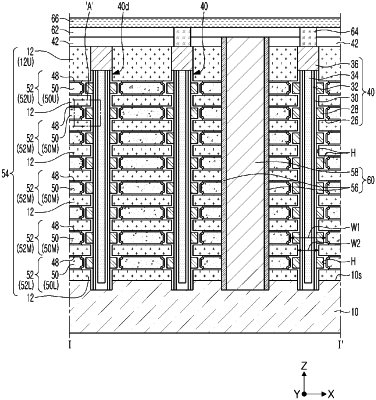
1. A semiconductor device comprising:
a lower structure;
a stacked structure on the lower structure and including a first interlayer insulating layer, a second interlayer insulating layer on the first interlayer insulating layer and a cell gate pattern between the first and second interlayer insulating layers;
a separation structure penetrating through the stacked structure; and
a memory vertical structure penetrating through the stacked structure,
wherein the memory vertical structure includes a first portion located on a same level as a level of the cell gate pattern and second portions located on a same level as a level of the first and second interlayer insulating layers,
wherein each of the second portions has a width smaller than a width of the first portion,
wherein the memory vertical structure includes a first dielectric layer and a second dielectric layer, in contact with each other in the second portions, extended toward the first portion, and spaced apart from each other in the first portion,
wherein the memory vertical structure further includes a data storage pattern disposed between the first dielectric layer and the second dielectric layer in the first portion,
wherein the first dielectric layer contacts the cell gate pattern and the first and second insulating layers,
wherein the cell gate pattern includes an upper surface contacting the second insulating layer, a lower surface contacting the first insulating layer and a first side contacting the first dielectric layer and a second side contacting the separation structure, and
wherein the first side of the cell gate pattern includes:
a central protruding portion protruding in a direction toward the first portion of the memory vertical structure in the cell gate pattern;
a first edge protruding portion adjacent to the first interlayer insulating layer;
a second edge protruding portion adjacent to the second interlayer insulating layer;
a first recess portion between the central protruding portion and the first edge protruding portion; and
a second recess portion between the central protruding portion and the first edge protruding portion.
|