| CPC H01L 29/41708 (2013.01) [H01L 27/0664 (2013.01); H01L 29/1095 (2013.01); H01L 29/407 (2013.01); H01L 29/45 (2013.01); H01L 29/7397 (2013.01); H01L 29/8613 (2013.01)] | 14 Claims |
|
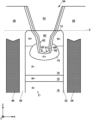
1. A semiconductor device comprising:
a drift region of first conductivity type provided in a semiconductor substrate;
a base region of second conductivity type provided in the semiconductor substrate;
an emitter region of first conductivity type provided at a front surface of the semiconductor substrate;
a contact region of second conductivity type provided on the base region and having a higher doping concentration than the base region;
a contact trench portion provided at the front surface of the semiconductor substrate;
a first barrier layer provided at a side wall and a bottom surface of the contact trench portion; and
a second barrier layer provided in contact with the contact region at the side wall of the contact trench portion, wherein
the second barrier layer is a silicon oxide film, and
a contact resistance between the second barrier layer and the emitter region is 100Ω or less.
|