| CPC H01L 27/14647 (2013.01) [H01L 27/14607 (2013.01); H01L 27/14614 (2013.01); H01L 27/14636 (2013.01); H01L 27/1464 (2013.01)] | 13 Claims |
|
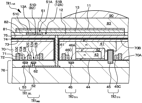
1. A light detecting device, comprising:
a semiconductor substrate;
a first photoelectric conversion section disposed above the semiconductor substrate, the first photoelectric conversion section comprising:
a first electrode;
a second electrode; and
a first photoelectric conversion layer disposed between the first electrode and the second electrode; and
a second photoelectric conversion section disposed above the first photoelectric conversion section, the second photoelectric conversion section comprising:
a third electrode;
a fourth electrode;
a second photoelectric conversion layer disposed between the third electrode and the fourth electrode; and
a first transistor electrically coupled to one of the third electrode and the fourth electrode.
|