US 11,699,716 B2
Solid-state imaging device
Kenji Kobayashi, Kanagawa (JP); Toshifumi Wakano, Kanagawa (JP); and Yusuke Otake, Kanagawa (JP)
Assigned to SONY SEMICONDUCTOR SOLUTIONS CORPORATION, Kanagawa (JP)
Filed by SONY SEMICONDUCTOR SOLUTIONS CORPORATION, Kanagawa (JP)
Filed on Nov. 15, 2021, as Appl. No. 17/526,800.
Application 17/526,800 is a continuation of application No. 16/803,787, filed on Feb. 27, 2020, granted, now 11,222,916.
Application 16/803,787 is a continuation of application No. 16/326,060, granted, now 10,680,028, issued on Jul. 25, 2018, previously published as PCT/JP2018/027845, filed on Jul. 25, 2018.
Claims priority of application No. 2017-151980 (JP), filed on Aug. 4, 2017.
Prior Publication US 2022/0077218 A1, Mar. 10, 2022
This patent is subject to a terminal disclaimer.
Int. Cl. H01L 27/146 (2006.01); H01L 23/522 (2006.01); H01L 31/107 (2006.01)
CPC H01L 27/14636 (2013.01) [H01L 23/5225 (2013.01); H01L 27/1464 (2013.01); H01L 27/14603 (2013.01); H01L 27/14634 (2013.01); H01L 31/107 (2013.01)] 19 Claims
OG exemplary drawing
 
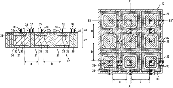
1. A light detecting device, comprising:
a first pixel and a second pixel, the first pixel including a first semiconductor region and a second semiconductor region, the second pixel including a third semiconductor region and a fourth semiconductor region; and
a first wiring layer including:
a first electrode;
a first via coupled to the first electrode and the first semiconductor region; and
a second via coupled to the first electrode and the third semiconductor region,
wherein a conductivity type of the first semiconductor region is opposite to a conductivity type of the second semiconductor region.