US 11,699,712 B2
Solid-state imaging device with layered microlenses and method for manufacturing same
Yoichi Ootsuka, Kumamoto (JP); Tomoyuki Yamashita, Kumamoto (JP); Kiyotaka Tabuchi, Kumamoto (JP); Yoshinori Toumiya, Kumamoto (JP); and Akiko Ogino, Kumamoto (JP)
Assigned to Sony Group Corporation, Tokyo (JP)
Filed by Sony Group Corporation, Tokyo (JP)
Filed on Dec. 6, 2021, as Appl. No. 17/543,590.
Application 17/543,590 is a continuation of application No. 16/440,684, filed on Jun. 13, 2019, granted, now 11,211,417.
Application 16/440,684 is a continuation of application No. 15/653,819, filed on Jul. 19, 2017, granted, now 10,355,038.
Application 15/653,819 is a continuation of application No. 14/861,175, filed on Sep. 22, 2015, granted, now 9,741,757.
Application 14/861,175 is a continuation of application No. 13/613,261, filed on Sep. 13, 2012, granted, now 9,159,760.
Claims priority of application No. 2011-217423 (JP), filed on Sep. 30, 2011.
Prior Publication US 2022/0093670 A1, Mar. 24, 2022
Int. Cl. H01L 27/14 (2006.01); H01L 27/146 (2006.01); H04N 25/00 (2023.01)
CPC H01L 27/14627 (2013.01) [H01L 27/14612 (2013.01); H01L 27/14621 (2013.01); H01L 27/14685 (2013.01); H04N 25/00 (2023.01)] 21 Claims
OG exemplary drawing
 
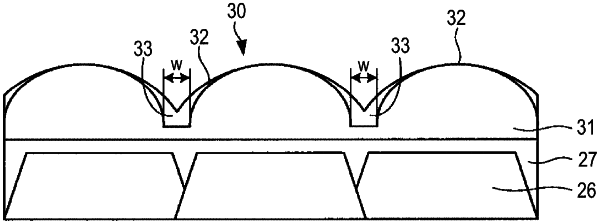
1. An imaging device comprising a micro lens comprising:
a first lens layer comprising a plurality of first micro lenses with inter pixel gaps therebetween; and
a second lens layer above the first lens layer;
wherein a thickness of the second lens layer at a central portion of one of the first micro lenses in the plurality of first micro lenses is less than a thickness of the second lens layer at a periphery of the one of the first micro lenses and throughout an inter pixel gap; and
wherein an inter pixel gap in an opposite side direction is smaller than an inter pixel gap in a diagonal direction.