| CPC H01L 27/14627 (2013.01) | 19 Claims |
|
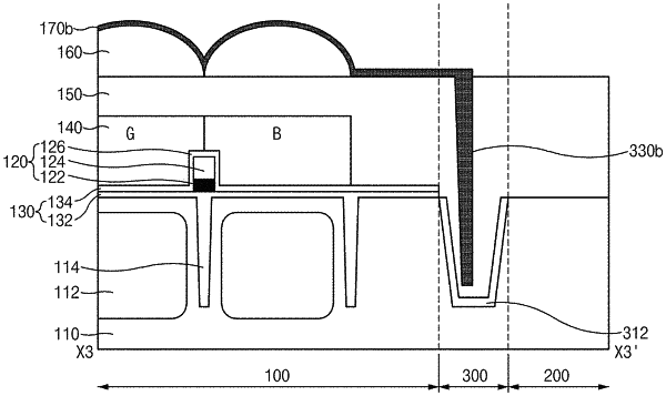
1. An image sensing device comprising:
a semiconductor substrate structured to include a pixel region, which includes a plurality of unit pixels, and a pixel-array peripheral region located outside of and peripheral to the pixel region;
a material layer disposed over the semiconductor substrate in the pixel region and the pixel-array peripheral region, and structured to include a first trench extending to a predetermined depth in the pixel-array peripheral region;
a lens layer disposed over the material layer in the pixel region and structured as a lens for collecting incident light into a unit pixel in the pixel region; and
a lens capping layer disposed over the lens layer and the material layer and structured to include an edge region formed to fill the first trench.
|