US 11,699,704 B2
Monolithic integration of a thin film transistor over a complimentary transistor
Van H. Le, Portland, OR (US); Marko Radosavljevic, Portland, OR (US); Han Wui Then, Portland, OR (US); Willy Rachmady, Beaverton, OR (US); Ravi Pillarisetty, Portland, OR (US); Abhishek Sharma, Hillsboro, OR (US); Gilbert Dewey, Hillsboro, OR (US); and Sansaptak Dasgupta, Hillsboro, OR (US)
Assigned to INTEL CORPORATION, Santa Clara, CA (US)
Appl. No. 16/642,356
Filed by Intel Corporation, Santa Clara, CA (US)
PCT Filed Sep. 28, 2017, PCT No. PCT/US2017/054144
§ 371(c)(1), (2) Date Feb. 26, 2020,
PCT Pub. No. WO2019/066872, PCT Pub. Date Apr. 4, 2019.
Prior Publication US 2021/0074702 A1, Mar. 11, 2021
Int. Cl. H01L 27/092 (2006.01); H01L 21/8258 (2006.01); H01L 27/088 (2006.01); H01L 29/20 (2006.01); H01L 29/205 (2006.01); H01L 29/66 (2006.01); H01L 29/778 (2006.01); H01L 29/786 (2006.01)
CPC H01L 27/0922 (2013.01) [H01L 21/8258 (2013.01); H01L 27/0883 (2013.01); H01L 29/2003 (2013.01); H01L 29/205 (2013.01); H01L 29/66462 (2013.01); H01L 29/66969 (2013.01); H01L 29/7786 (2013.01); H01L 29/7869 (2013.01)] 20 Claims
OG exemplary drawing
 
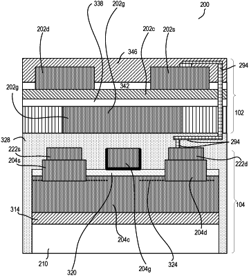
1. An apparatus comprising:
a first device comprising an enhancement mode III-N heterostructure field effect transistor (HFET);
a second device over the first device, wherein the second device comprises a depletion mode thin film transistor, wherein the second device includes a layer comprising an oxide semiconductor extending laterally from a source terminal of the second device to a drain terminal of the second device, and a gate stack coupled to the layer; and
a connector to couple a source terminal of the first device to the drain terminal of the second device, or couple a drain terminal of the first device to the source terminal of the second device.