| CPC H01L 27/0886 (2013.01) [H01L 29/42392 (2013.01); H01L 29/785 (2013.01); H01L 29/78696 (2013.01)] | 20 Claims |

|
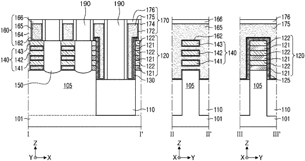
1. A method of manufacturing a semiconductor device, the method comprising:
forming first layers and second layers by alternately stacking the first layers and the second layers on a substrate;
forming an active structure extending in a direction parallel to an upper surface of the substrate by removing a portion of the substrate and a stacked structure of the first layers and the second layers;
forming a blocking layer covering at least one end portion of the active structure;
forming sacrificial gate structures on the active structure and the blocking layer;
forming recess regions by removing the first layers and the second layers exposed between the sacrificial gate structures;
forming source/drain regions on the recess regions;
forming an interlayer insulating layer on the source/drain regions;
forming gap regions by removing the sacrificial gate structures and the first layers;
forming gate structures by depositing a gate dielectric layer and a gate electrode in the gap regions; and
forming contact plugs connected to the source/drain regions through the interlayer insulating layer,
wherein an etchant for removing the first layers is blocked by the blocking layer so that the at least one end portion of the active structure is protected from the etchant.
|