| CPC H01L 27/0262 (2013.01) | 8 Claims |

|
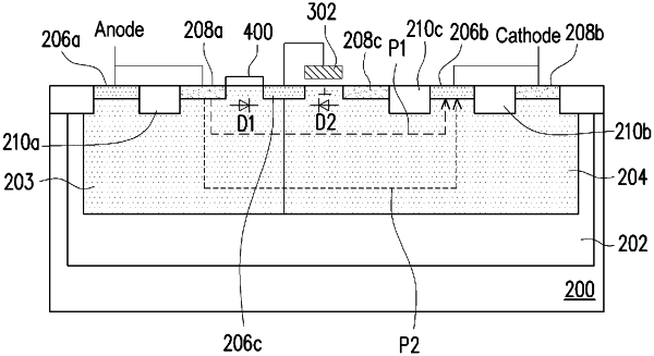
1. A silicon-controlled rectifier, comprising:
a substrate of a first conductivity type;
a deep well region of a second conductivity type, formed in the substrate;
a well region of the first conductivity type and a well region of the second conductivity type, formed side by side in the deep well region;
wherein a first heavily doped active region of the second conductivity type and a first heavily doped active region of the first conductivity type are disposed in the well region of the second conductivity type, the first heavily doped active region of the second conductivity type and the first heavily doped active region of the first conductivity type are both connected to an anode, and a first shallow trench isolation structure is disposed in between the two;
a second heavily doped active region of the second conductivity type and a second heavily doped active region of first conductivity type are disposed in the well region of the first conductivity type, the second heavily doped active region of the second conductivity type and the second heavily doped active region of the first conductivity type are both connected to a cathode, and a second shallow trench isolation structure is disposed in between the two;
a third heavily doped active region of the second conductivity type, shared across the well region of the first conductivity type and the well region of the second conductivity type, wherein the third heavily doped active region of the second conductivity type is separated from the first heavily doped active region of the first conductivity type by a first distance, and a forward diode is formed in the first heavily doped active region of the first conductivity type and the well region of the second conductivity type; and
a third heavily doped active region of the first conductivity type, disposed in the well region of the first conductivity type provided between the second heavily doped active region of the second conductivity type and the third heavily doped active region of the second conductivity type, wherein a third shallow trench isolation structure is disposed in between the second heavily doped active region of the second conductivity type and the third heavily doped active region of the first conductivity type, the third heavily doped active region of second conductivity type is separated from the third heavily doped active region of first conductivity type by a second distance, and a reverse diode is formed in the third heavily doped active region of the second conductivity type and the well region of the first conductivity.
|