| CPC H01L 27/0207 (2013.01) [H01L 23/481 (2013.01); H01L 23/5223 (2013.01); G06F 30/392 (2020.01)] | 12 Claims |
|
1. A semiconductor device comprising:
a first integrated circuit and a second integrated circuit disposed on a semiconductor substrate and spaced apart from each other;
a wiring structure disposed on the semiconductor substrate and configured to electrically connect the first integrated circuit and the second integrated circuit; and
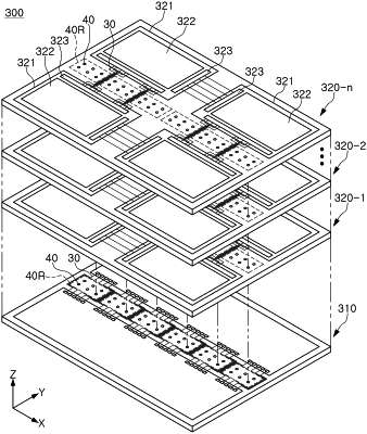
a first TSV area and a second TSV area disposed between the first integrated circuit and the second integrated circuit, and including a plurality of first and second TSV structures penetrating through the semiconductor substrate, respectively,
wherein, on a plane, the semiconductor substrate has a TSV array region disposed between the first integrated circuit and the second integrated circuit, and extending in a first direction,
wherein, on the plane, the first TSV area and the second TSV area are spaced apart from each other in the first direction within the TSV array region, and
wherein on the plane the wiring structure extends from the first integrated circuit to the second integrated circuit and passes between the first TSV area and the second TSV area in a second direction perpendicular to the first direction.
|