| CPC H01L 25/18 (2013.01) [H01L 24/05 (2013.01); H01L 24/08 (2013.01); H01L 25/0657 (2013.01); H01L 2224/05147 (2013.01); H01L 2224/08145 (2013.01); H01L 2924/1431 (2013.01); H01L 2924/14511 (2013.01)] | 20 Claims |
|
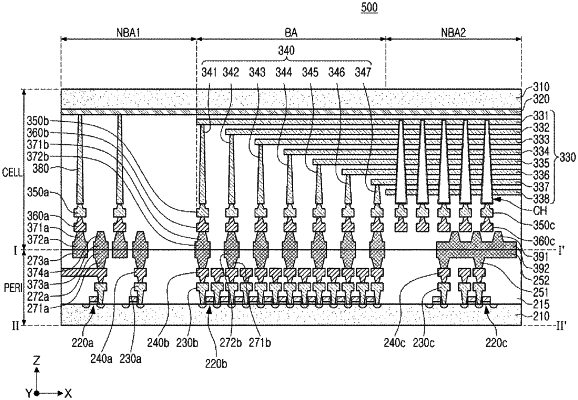
1. A memory device comprising:
a first chip configured to include a memory cell array disposed on a first substrate, and a plurality of first metal pads on a first uppermost metal layer of the first chip; and
a second chip configured to include peripheral circuits disposed on a second substrate, and a plurality of second metal pads on a second uppermost metal layer of the second chip, the peripheral circuits operating the memory cell array,
wherein at least one of the plurality of first metal pads of the first chip and at least one of the plurality of second metal pads of the second chip are connected in a first area, the at least one of the plurality of first metal pads being connected to the memory cell array and the at least one of the plurality of second metal pads being connected to the peripheral circuits, and
wherein a further at least one of the plurality of first metal pads of the first chip and a further at least one of the plurality of second metal pads of the second chip are connected in a second area, the further at least one of the plurality of first metal pads being not connected to the memory cell array and the further at least one of the plurality of second metal pads being connected to the peripheral circuits, and
wherein the further at least one of the plurality of second metal pads forms a power routing wire used for supplying power to the peripheral circuits of the second chip.
|