| CPC H01L 25/0657 (2013.01) [H01L 23/13 (2013.01); H01L 23/367 (2013.01); H01L 23/49833 (2013.01); H01L 23/49838 (2013.01); H01L 24/14 (2013.01); H01L 25/18 (2013.01); H01L 2224/14519 (2013.01); H01L 2225/06513 (2013.01); H01L 2225/06517 (2013.01); H01L 2225/06541 (2013.01); H01L 2225/06586 (2013.01); H01L 2225/06589 (2013.01); H01L 2924/1431 (2013.01); H01L 2924/1434 (2013.01)] | 16 Claims |
|
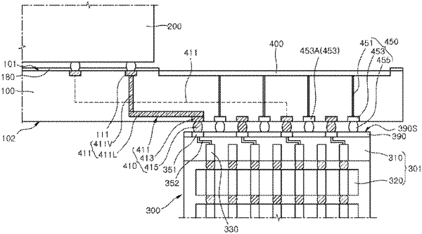
1. A semiconductor package comprising:
an interposer including first and second surfaces opposite to each other;
a heat dissipation layer disposed on the first surface of the interposer;
a first semiconductor die mounted on the first surface of the interposer;
a stack of second semiconductor dies mounted on the second surface of the interposer; and
a thermally conductive connection part for transferring heat from the stack of the second semiconductor dies to the heat dissipation layer,
wherein the interposer further includes a passivation layer exposing a surface of the heat dissipation layer on the first surface of the interposer.
|