| CPC H01L 25/0655 (2013.01) [H01L 21/565 (2013.01); H01L 23/13 (2013.01); H01L 23/31 (2013.01)] | 19 Claims |
|
1. A semiconductor package comprising:
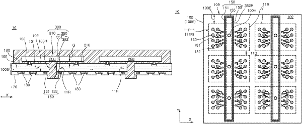
a package substrate with vent holes formed therethrough;
semiconductor chips disposed on the package substrate; and
a molding layer including an upper molding portion that encapsulates the semiconductor chips, and a lower molding portion that is connected to the upper molding portion through the vent holes,
wherein the package substrate includes:
a substrate body including a plurality of unit regions with the vent holes disposed therethrough;
ball lands disposed in each of the unit regions of the substrate body;
first and second dam patterns that are spaced apart from the ball lands of the substrate body, extending across the unit regions and further extending into edge regions of the substrate body, which is outside of the unit regions, and
a dielectric layer that extends to cover the substrate body, the first and second dam patterns being covered and some portions of the ball lands being opened by the dielectric layer.
|