| CPC H01L 25/0652 (2013.01) [H01L 21/32 (2013.01); H01L 23/3128 (2013.01); H01L 24/73 (2013.01); H01L 2224/32145 (2013.01); H01L 2224/32225 (2013.01); H01L 2224/73265 (2013.01); H01L 2225/0651 (2013.01); H01L 2225/06506 (2013.01); H01L 2225/06562 (2013.01); H01L 2225/06572 (2013.01)] | 20 Claims |
|
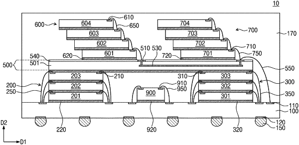
1. A semiconductor package, comprising:
a substrate;
a first lower stack on the substrate, the first lower stack including a plurality of first lower semiconductor chips stacked on each other;
a redistribution substrate on the first lower stack;
a redistribution connector on the substrate, the redistribution connector electrically connecting the substrate to the redistribution substrate;
a first upper stack on the redistribution substrate, the first upper stack including a plurality of first upper semiconductor chips stacked in a cascade formation;
a first upper connector on the redistribution substrate, the first upper connector electrically connecting the redistribution substrate to the first upper stack;
a second upper stack on the redistribution substrate and horizontally spaced apart from the first upper stack, the second upper stack including a plurality of second upper semiconductor chips stacked in a cascade formation; and
a second upper connector on the redistribution substrate, the second upper connector electrically connecting the redistribution substrate to the second upper stack,
wherein the redistribution connector is on one side edge at a top surface of the redistribution substrate, the top surface of the redistribution substrate being a surface on which the first upper stack and the second upper stack are provided,
wherein the first upper connector is on one side edge at a top surface of the first upper stack, and
wherein the second upper connector is on one side edge at a top surface of the second upper stack.
|