| CPC H01L 23/552 (2013.01) [H01L 23/3121 (2013.01); H01L 23/49575 (2013.01); H01L 24/32 (2013.01); H01L 25/0657 (2013.01); H05K 1/0218 (2013.01); H01L 2224/32145 (2013.01); H01L 2224/32225 (2013.01); H01L 2224/32245 (2013.01); H05K 2201/10371 (2013.01)] | 20 Claims |
|
1. A semiconductor module comprising:
a main board;
a plurality of external terminals disposed on an upper surface of the main board;
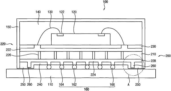
a package substrate including a core insulation layer, a conductive pattern disposed on the core insulation layer and configured to be electrically connected with the plurality of external terminals, an upper insulation pattern and a lower insulation pattern, the upper insulation pattern is disposed on an upper surface of the core insulation layer and partially exposes the conductive pattern, and the lower insulation pattern is disposed on a lower surface of the core insulation layer and partially exposes the conductive pattern;
at least one semiconductor chip disposed on an upper surface of the package substrate and configured to be electrically connected with the conductive pattern;
a molding member disposed on the upper surface of the package substrate and covering the at least one semiconductor chip; and
a shielding plate disposed on an upper surface and lateral side surfaces of the molding member and lateral side surfaces of the package substrate and configured to shield electromagnetic interference (EMI) emitted from the at least one semiconductor chip,
a shielding fence that extends from an edge portion of a lower surface of the lower insulation pattern, the shielding fence directly contacting the upper surface of the main board, the shielding fence surrounds the external terminals and is configured to shield EMI emitted from the plurality of external terminals, and
a reinforcing member disposed in the shielding fence and configured to increase a strength of the shielding fence.
|