| CPC H01L 23/5226 (2013.01) [H01L 21/486 (2013.01); H01L 22/12 (2013.01); H01L 23/31 (2013.01); H01L 24/14 (2013.01); H01L 2224/023 (2013.01); H01L 2224/0401 (2013.01)] | 20 Claims |
|
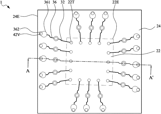
1. An electronic device package, comprising:
an encapsulated electronic component;
a redistribution layer (RDL) disposed above the encapsulated electronic component, wherein the RDL comprises a circuit layer comprising a conductive pad including a pad portion having a curved edge and a center of curvature, and an extension portion protruding from the pad portion and having a curved edge and a center of curvature; and
a conductive via comprising a connection region connected to the conductive pad of the RDL,
wherein a center of the connection region of the conductive via is closer to the center of curvature of the edge of the extension portion than to the center of curvature of the edge of the pad portion.
|