| CPC H01L 23/49827 (2013.01) [H01L 21/486 (2013.01); H01L 23/552 (2013.01)] | 16 Claims |
|
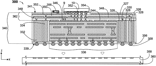
1. An integrated-circuit package assembly, comprising:
an integrated-circuit (IC) package substrate, including a die side and a land side;
a plurality of interconnects located at a periphery of the package substrate, including:
an input/output interconnect that extends at least the height of the IC package land side to a redistribution layer near the IC package die side, wherein the input/output interconnect is shielded by a ground (Vss) annulus;
a power interconnect that extends at least the height of the IC package land side to the redistribution layer near the IC package die side, wherein the power interconnect is shielded by a ground (Vss) annulus;
wherein the redistribution layer is coupled to each of the IC package substrate, the input/output interconnect and the power interconnect.
|