| CPC H01L 23/49822 (2013.01) [H01L 21/486 (2013.01); H01L 21/4857 (2013.01); H01L 21/568 (2013.01); H01L 23/3128 (2013.01); H01L 23/49827 (2013.01); H01L 23/528 (2013.01); H01L 23/5226 (2013.01); H01L 24/18 (2013.01); H01L 2224/16225 (2013.01); H01L 2224/18 (2013.01); H01L 2224/32225 (2013.01); H01L 2224/73204 (2013.01); H01L 2924/15311 (2013.01); H01L 2924/181 (2013.01)] | 12 Claims |
|
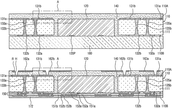
1. A method for manufacturing a semiconductor package, the method comprising:
disposing a semiconductor chip having contact pads, and a connection structure around the semiconductor chip on a supporting substrate, with the contact pads facing the supporting substrate;
forming an encapsulant encapsulating the semiconductor chip and the connection structure on the supporting substrate;
embedding a wiring pattern having a connection portion in the encapsulant, the connection portion having a connection hole;
forming a through hole penetrating the encapsulant in the connection hole, the through hole exposing a portion of an upper surface of the connection structure; and
forming a conductive via in the through hole, the conductive via connecting the wiring pattern to the connection structure.
|
|
8. A method for manufacturing a semiconductor package, the method comprising:
preparing a package structure comprising a connection member including a first redistribution layer, a semiconductor chip having disposed on the connection member, a connection structure disposed around the semiconductor chip on the connection member, and an encapsulant encapsulating the semiconductor chip and the connection structure on the connection member, the first redistribution layer electrically connecting the semiconductor chip and a lower surface of the connection structure:
embedding a wiring pattern having a connection portion in the encapsulant, the connection portion having a connection hole;
forming a through hole penetrating the encapsulant in the connection hole, the through hole exposing a portion of an upper surface of the connection structure; and
forming a conductive via in the through hole, the conductive via connecting the wiring pattern to the connection structure.
|