| CPC H01L 23/49816 (2013.01) [H01L 23/3114 (2013.01); H01L 23/49861 (2013.01); H01L 24/13 (2013.01)] | 19 Claims |
|
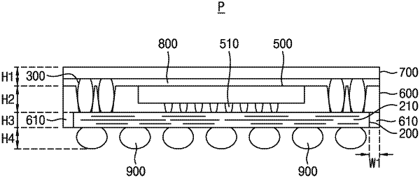
1. A semiconductor package comprising:
a redistribution layer;
a semiconductor chip electrically connected to the redistribution layer, and disposed on an upper surface of the redistribution layer;
a plurality of solder balls disposed on the upper surface of the redistribution layer spaced apart from the semiconductor chip and electrically connected to the redistribution layer;
an interposer electrically connected to the plurality of solder balls, and disposed directly on upper surfaces of the plurality of solder balls;
an encapsulant layer encapsulating the semiconductor chip, and side surfaces and a portion of the upper surface of the redistribution layer under the interposer; and
an underfill layer filling a space between a lower surface of the interposer and an upper surface of the encapsulant layer,
wherein the encapsulant layer includes a side surface encapsulant region surrounding the side surfaces of the redistribution layer, and a first region surrounding the semiconductor chip and covering the upper surface of the redistribution layer,
wherein the side surface encapsulant region and the first region are continuously integrated with each other without a boundary therebetween and integrally formed through a single process,
wherein the underfill layer contacts the lower surface of the interposer, the upper surface of the encapsulant layer, an upper surface of the semiconductor chip, and side surfaces of the plurality of solder balls, and
wherein upper portions of the plurality of solder balls are surrounded by the underfill layer and lower portions of the plurality of solder balls are surrounded by the encapsulant layer and contact the encapsulant layer.
|