| CPC H01L 23/49537 (2013.01) [H01L 21/4825 (2013.01); H01L 21/4842 (2013.01); H01L 23/49524 (2013.01); H01L 24/33 (2013.01); H01L 24/83 (2013.01); H01L 24/97 (2013.01); H05K 1/185 (2013.01); H01L 23/49513 (2013.01); H01L 24/05 (2013.01); H01L 24/06 (2013.01); H01L 24/32 (2013.01); H01L 2224/05647 (2013.01); H01L 2224/06181 (2013.01); H01L 2224/32245 (2013.01); H01L 2224/33181 (2013.01); H01L 2224/83203 (2013.01); H01L 2224/83385 (2013.01); H01L 2224/83815 (2013.01); H05K 3/0035 (2013.01); H05K 3/0038 (2013.01); H05K 3/0047 (2013.01)] | 17 Claims |
|
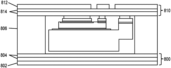
1. A method of batch producing power modules, the method comprising:
applying a first solder paste to substrate sections of a leadframe structure, wherein each substrate section belongs to a different one of the power modules;
placing a power semiconductor die on the first solder paste of each substrate section, each power semiconductor die having a first load terminal and a control terminal at a first side that faces away from the leadframe structure and a second load terminal contacting the first solder paste at a second side opposite the first side;
applying a second solder paste to the first load terminal and the control terminal of each power semiconductor die;
vertically aligning a metal clip frame with the leadframe structure, the metal clip frame comprising a first metal clip vertically aligned with the first load terminal of each power semiconductor die and a second metal clip vertically aligned with the control terminal of each power semiconductor die;
pressing the metal clip frame toward the leadframe structure in a pressing direction, wherein a hard stop feature prevents further pressing when the hard stop feature is engaged;
reflowing the first solder paste and the second solder paste to form a first soldered joint between each first metal clip and the corresponding first load terminal of each power semiconductor die, a second soldered joint between each second metal clip and the corresponding control terminal of each power semiconductor die, and a third soldered joint between the second load terminal of each power semiconductor die and the corresponding substrate section of the leadframe structure; and
severing connections to the leadframe structure and to the metal clip frame, to form individual power modules.
|